Computer Memory Part 1

Oskar Mendel
Posted on June 14, 2022

At work, we have something that we call "competence day" once per month where all developers spend an entire day learning new things and keeping up to date with technology. Recently I've been spending those days just reading since when working a day job then coming home coding at Nullsson things I rarely have time left to read.
Inspired by a talk that Jonathan Blow had called "Preventing the collapse of civilization" I started to investigate academic papers since that's an area that I have usually avoided in the past. Within this talk Jonathan mentions how technology degrades naturally and this has since stuck with me. I notice just with smaller features at work that while working on a feature you become sort of an expert at that specific thing since you're investigating and falling down all the different pits there is implementing that thing. If someone else would pick up your work mid through they'd have to go through the same process and potentially making the same mistakes you did.
I stumbled upon a paper by a man named Ulrich Drepper called "What Every Programmer Should Know About Memory" and this paper was sort of a big eye opener for me. It inspired me to make a presentation at work teaching others about what I've learned and that is also what this initial article is about, my notes learning about this stuff.
For me there are several areas of memory I want to explore and I plan on making this series about the things I learn researching this and learning more about it. I plan on doing a few of these depending on how interesting and valuable I feel it is.
Computers
Historically computers were first designed as a single component where all components had a similar performance. Later this was split up into different components and optimized which resulted in some parts being faster than others. This also resulted in some components becoming bottlenecks, the main ones was and still is the mass storage and memory systems. Since we are going through memory with these articles we will completely ignore the mass storage part just like Ulrich's paper.
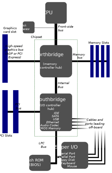
By Original: Gribeco at French WikipediaDerivative work: Moxfyre at English Wikipedia - This file was derived from: Diagramme carte mère.png, CC BY-SA 3.0, https://commons.wikimedia.org/w/index.php?curid=3789066
Personal computers and smaller servers adopted a structure where the chip was split into two main parts: The northbridge and the southbridge. This today has changed a bit but I feel like its still relevant when we think about how things works.
The CPU was connected to the northbridge through what's called the front side bus also known as FSB. Inside the northbridge there is a memory controller whose implementation decides which types of RAM chips that are supported by the computer.
To reach other system devices the northbridge communicates with the southbridge which in turn communicates with different devices through its own set of busses like PCI, PCI Express, SATA and USB.
Historically this design came with a problem which was when a device wants to access the RAM. In older PCs' communication on either bridge had to pass through the CPU which resulted in performance problems. A workaround was developed called DMA (Direct memory access). DMA allowed the northbridge to help store and receive data in RAM directly. This is what basically all high performance devices use today and the battle is for bandwidth since the northbridge and CPU compete for RAM access.
Other components on the chip such as the network controller cannot really afford all the traffic passing the CPU either hence it makes heavy use of DMA by writing and reading memory there directly. At times where there is heavy DMA traffic it might stall the CPU just because its waiting for data from the memory. Worth to note that today the northbridge has been moved into the CPU itself on modern chips and instead we just refer to it as CPU and a chipset where the chipset acts like a southbridge.
Different types of RAM
RAM stands for "Random Access Memory" and what this means is that memory doesn't have to be accessed in a sequence and instead can be accessed directly. There are several different types of RAM and the differences can be dramatic, we will however keep it on topic and only talk about the main ones being SRAM (Static RAM) and DRAM (Dynamic RAM).
Hardware intermission
Before getting into the specifics I feel like its important to understand the two main electrical components that we will talk about moving forward. First of all we got the Transistor which is the main component in almost any electrical devices today.
A transistor is like a binary switch which allows current to either flow through it or not, they can be placed in different patterns to form logical gates.
Then we have the Capacitor which is a component used to store a small electrical charge and release it at a later time. I picture this almost like a very small battery.
These components today are made at semiconductor using technology that allows to make these components in the size of nanometers. This is so small that you can't see it without a microscope.
Static RAM
Taken from Drepper, Ulrich. “What Every Programmer Should Know About Memory.” (2007).
This is a 6 transistor static RAM cell. The core of it is made up of M1 - M4 which forms two "Cross Coupled Inverters". They can have two stable states either 0 or 1 respectively and they are stable for as long as there is power available on the Vdd (Voltage Drain Drain). These are used as a sort of "Flip Flop" mechanism to flip the electrical current back and forth to avoid having to refresh the state which we will get into shortly. In order to access its state the WL (Word Access Line) is raised which allows the state of the cell to immediately be available on the two BL lines.
Dynamic RAM

Taken from Drepper, Ulrich. “What Every Programmer Should Know About Memory.” (2007).
Here is a dynamic RAM cell which you can probably see looks simpler than the static one. This is because it only uses one transistor and one capacitor. The state of the cell is kept within the capacitor in form of an electric charge and the transistor is used to guard the access to it.
In order to read the state of the cell the Access Line (AL) is raised which causes current to flow on the Data Line (DL) or not depending on the capacitor. To write state to the cell the DL is set and then AL is raised for a long enough time to either charge or drain the capacitor. An important thing to keep in mind here is that since the cell makes use of a capacitor the charge inside it is drained every time its state is read. This means you cannot repeat the procedure without charging it somehow. Every read of a cell is followed by a write where the output of the read is routed back to the cell to automatically charge it again.
It only takes a short amount of time to charge the cell but also for the charge to dissipate and this problem is referred to as "Leakage". A RAM cell like this can store one bit for us (0 or 1) and today it is common with several gigabytes of RAM storage on these chips hence we are talking billions of these cells and because of leakage all of their state has to be refreshed. For most chips this needs to happen every 64ms. During a refresh it is not possible to access the memory, the reason behind this is that a refresh is basically a read operation where the read value is immediately discarded. For some workloads this overhead may stall up to 50% of the memory access.
The main advantage that the dynamic RAM cells have over static RAM is the chip real estate. DRAM cells takes up much less space but is also much cheaper to produce. This means its simpler to pack several of them close together on the same die. SRAM cells are mainly used for our CPU caches.
DRAM Access
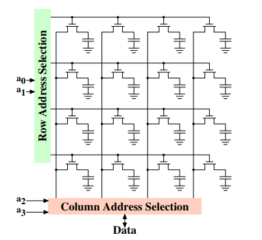
A program that we developers make uses virtual addresses for its memory locations, the CPU takes these virtual addresses and translates them to physical ones and finally the memory controller selects the RAM chip for that corresponding address. To select an individual memory cell on that RAM chip parts of the physical address are passed in the form of a number of address lines. Accessing memory individually from the memory controller is impractical since 4GB of RAM would require 2^32 address lines. Instead addresses is passed as an encoded binary number using a smaller set of address lines. This type of address needs to be demultiplexed first which means that one signal is routed into many signals (One to Many). The cells on the chip is organized in rows and columns in order to decrease the size of the demultiplexer.

Taken from Drepper, Ulrich. “What Every Programmer Should Know About Memory.” (2007).
First the Row Address Selection (RAS) is passed its signals which are demultiplexed in order to find the correct row for the address, when found the entire row of cells are made available to the Column Address Selection (CAS) which uses a multiplexer (Many to One) to route the correct cell to the data pin. Worth to note is that this happens several times in parallel.
DRAM Access technical details
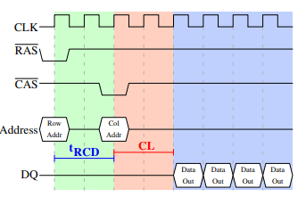
Synchronous DRAM (SDRAM) works relative to a clock provided by the memory controller which frequency determines the speed of the bus between the chips and memory controller. 800MHz, 1066MHz, 1333MHz and 1600MHz are all frequencies of used maybe 10 years ago. These frequencies used to advertise RAM chips are not the frequencies actually used on the bus but instead the values on the chips are double or quad pumped which means that the data is transported two respectively four times per cycle. A quad pumped 200MHz bus is therefore advertised as an effective 800MHz bus. However today it is not unusual for chips to be in the range of 3200 - 3800MHz.

Taken from Drepper, Ulrich. “What Every Programmer Should Know About Memory.” (2007).
A read cycle begins with the memory controller making the row address available by lowering the RAS signal. All signals are read on the rising edge of the CLK signal. Setting the row address causes the RAM chip to launch the addressed row. The CAS signal can be sent after a delay called RAS to CAS delay (tRCD) which is specified in clock cycles. The column address is then transmitted by making it available on the address bus and lowering the CAS line, this allows both the row and column address be sent on the same address bus. After this the addressing is complete and the data can be transmitted. The RAM chip needs some time to prepare for this and this is referred to as CAS latency (CL).
It is quite a process to read data as you can see. That is why it is important to try help the computer collect as much related data as possible in one go in order to not have to go through this process as much, this is one of the ideas behind "Data oriented design". The memory controller helps with the process by not only transferring one data word but instead DRAM modules allows the memory controller to specify how much data to be transmitted to save time, this is often a choice between 2, 4 or 8 words. This allows for filling entire cache lines without a new read cycle.
DDR is a technology that is used today which stands for Double Data Rate, this allows for data to be read on the rising edge of the CLK signal as well allowing data to be read at double the speed without an increase in frequency.
Thoughts
Just this first part learning about RAM and how the tech works was so fruitful. Like I said for me reading this for the first time was an eye opener when it comes to how powerful machines we have in front of us today. I did previously to learning about this understand that memory access was something that you had to think about for performance but after learning about this suddenly there is a reason behind the question WHY things are the way they are. This has been my notes collected from learning about RAM and in the future I plan on doing a write-up on different areas of memory. Almost all the content of this article can also be learned about within the paper mentioned at the beginning of the article but for me it helps writing about it and reasoning a bit behind it for it to really stick and perhaps someone may find this useful.
References
- https://www.youtube.com/watch?v=ZSRHeXYDLko
- https://people.freebsd.org/~lstewart/articles/cpumemory.pdf
- https://en.wikipedia.org/wiki/Northbridge_(computing)
- https://web.archive.org/web/20141023034856/https://www.intel.com/content/dam/www/public/us/en/documents/product-briefs/x99-chipset-brief.pdf
- https://en.wikipedia.org/wiki/System_on_a_chip
- https://www.electronicshub.org/multiplexer-and-demultiplexer/
- https://www.sciencedirect.com/topics/computer-science/static-random-access-memory
- https://www.pcmag.com/encyclopedia/term/transistor
- https://www.pcmag.com/encyclopedia/term/capacitor
- https://en.wikipedia.org/wiki/Semiconductor_industry
- https://en.wikipedia.org/wiki/5_nm_process

Posted on June 14, 2022
Join Our Newsletter. No Spam, Only the good stuff.
Sign up to receive the latest update from our blog.


